The question is can we use multiple os at a time.
Yes we can do it.....
But our requirements are a live cd image of any os that you want to use Live cd is nothing but at the boot time when we place the cd we can use the o
s without any modifications and if you like it you can inst
all if you want to.There are several live cd's.The main fault of it is the data won't be stored in
it because it is not occuping any place in your harddisk.It is just using the RAM(Random Access Memory).
The virtualbox is the software released my SunMicro Systems.This software provides a virtual system like environment.Here the software uses t
he features of your PC and it recreates a new virtual pc.Here you can save the information.It works well i have tested it.
You can downl0ad virtual box from this
link
Click the link and select the option which fits for your pc.
Here i am going to show everything step by step procedure .
How to use it?
The installation procedure:
first you have to have virtual box software or you can download it from the link give above
download it based on your system configuration.
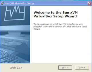
First step:
Double-click the downloaded sunvirtualbox software

Now we go to step 2
step 3:
click on next
step 4:
click i accept and click next
step 5:
 click next
step 6:

click next
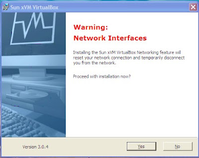
step 7:
click on yes this is used to make a lan like for the virtual box
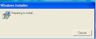
step 8:
step 10:
 This is will be displayed on the desktop during this work is going on don't double click untill the installation is completed
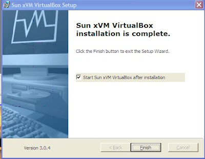
step 11:
click on finish
step 12:
step 13:
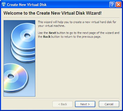
 click on new
step 14:
click on next
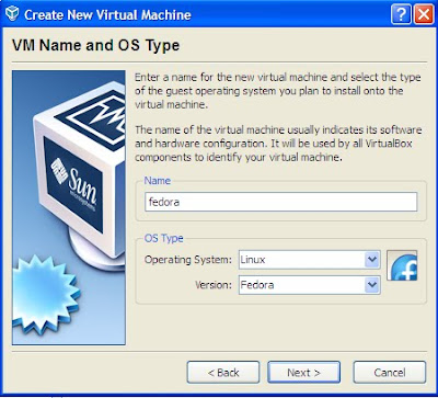
step 15:
type the name as your wish and os type
operating system as which you are using
and version as per yours
click on next
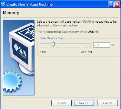
step 16:
set the ram half of your orginal ram if you have 1 gb ram then alocate to it less than 512 mb
click on next
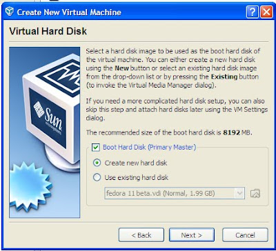
step 17:
click on create new harddisk and click on next
it creates your system memory as a seperate hard disk virtually it doesnot affect any of your system
step 18:
click on next
step 19:
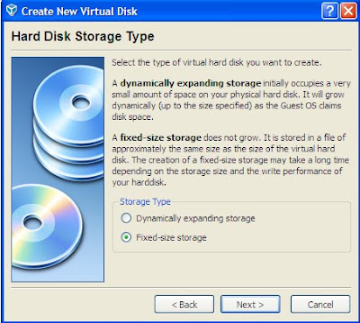
click on fixed size storage or dynamically expanding storage if you don't want to increase the size then fix to fixed size storage here i am showing fixed size storage
now click next
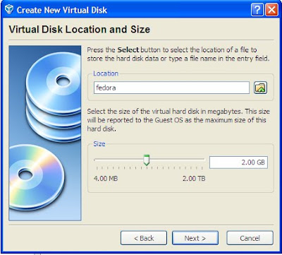
step 20:
here i am alocation 2gb as per which os i want to use i am using fedora live so i kept it as 2 gb for live cd's 2gb would be enough click on next
step 21:
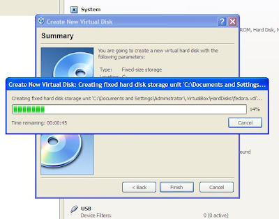
click on finish
step 22:
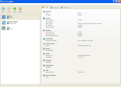
 it will be showing like this in the virtual box
powered off
and the name given at the beginning
step 23:
click on settings now
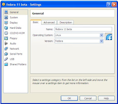
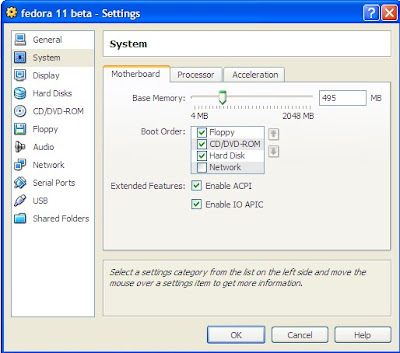
step 24:
now you will get like this window and here you need to keep the settings
now do everything as per figures
step 25:
step 26:
step 27:
step 28:
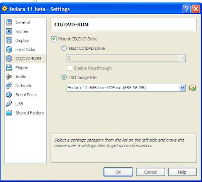
here in the above figure you should have a iso file of the live cd you have and you must browse it and show the location of it
step 29:
 step 30:
 step 31:
step 32:
 step 33:
step 34:
step 35:
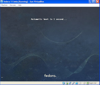
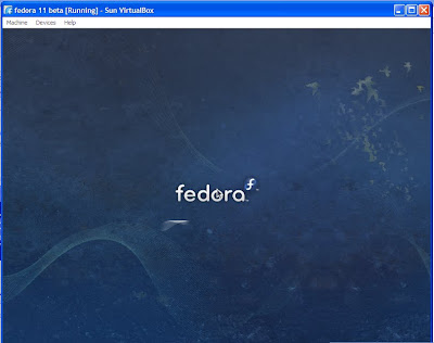
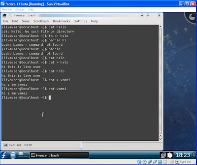
And now your are done but i will show that it works well
step 36:
step 37:
step 38:
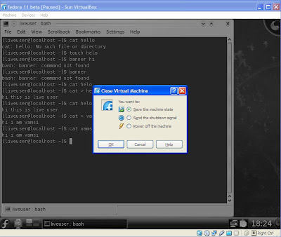
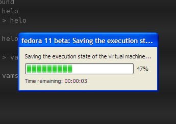
now here is the most important thing
when you are first using it just poweroff the machine do it for few times untill you get it correctly
and next time onwards you can save the machine state.
step 39:
step 40:
now you will see it like this
step 41:
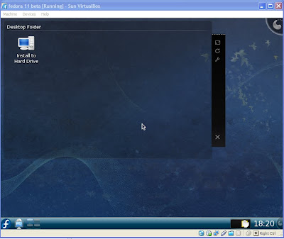
the final thing
is also the very beginning thing
select on the machine you want to start and click on start
If you get any kind of errors then just mail me
see my email id in my profile


